- 您现在的位置:买卖IC网 > Sheet目录1991 > CS4354-CSZ (Cirrus Logic Inc)IC DAC 24BIT SRL 14SOIC
DS895F2
11
CS4354
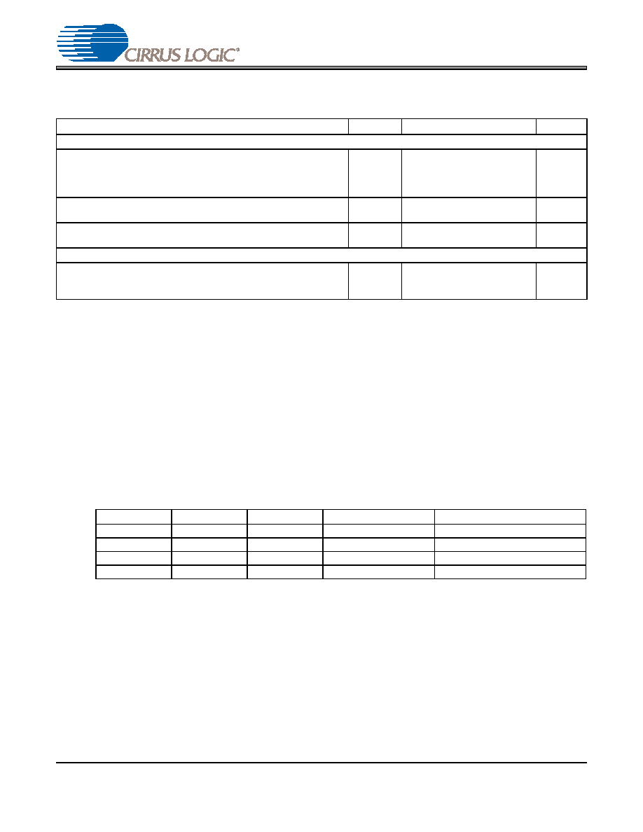
DC ELECTRICAL CHARACTERISTICS
Test conditions (unless otherwise specified): VA = 5 V, VL = 3.3 V; GND = 0 V; SDIN = 0; all voltages with respect
to ground.
Notes: 15. Power supply current increases with increasing sample rate and increasing MCLK frequency. Typical
values are based on Fs = 48 kHz and MCLK = 12.288 MHz. Maximum values are based on highest
sample rate and highest MCLK frequency; see “Switching Specifications - Serial Audio Interface” on
page 8. Variance between speed modes is small.
16. During normal operation, SDIN = 997 Hz sine wave at 0 dBFS with load resistance RL = 3 k.
17. Power-down is defined as all clock and data lines held static low. All digital inputs have a weak pull-
down (approximately 50 k
) which is only present during power on reset. Opposing this pull-down will
increase the power-down current.
18. Valid with the recommended capacitor values as shown in the “Typical Connection Diagram” on
2.1
Digital I/O Pin Characteristics
Input and output levels and associated typical power supply voltage are shown in Table 2. Logic levels
should not exceed the corresponding power supply voltage.
Table 2. Digital I/O Pin Characteristics
Parameters
Symbol
Min
Typ
Max
Units
Power Supplies
Power supply current (Note 15)
Normal operation (Note 16)
Power-down (Note 17)
IVA
IVL
IVA
IVL
-
10
0.1
0.5
1
13
0.2
-
mA
A
Power dissipation (all supplies)
Normal Operation (Note 16)
Power-Down (Note 17)
-
50
2.5
65
-
mW
Power supply rejection ratio (Note 18)
(1 kHz)
(60 Hz)
PSRR
-
60
-
dB
DC Output Voltages
Pin voltage
FILT+ to GND
FLYP to FLYN
GND to -VFILT
-
3.5
4.9
4.7
-
V
Pin Name
Power Supply
I/O
Driver
Receiver
MCLK
VL
Input
-
1.8 V - 5 V
LRCK
VL
Input
-
1.8 V - 5 V
SCLK
VL
Input
-
1.8 V - 5 V
SDIN
VL
Input
-
1.8 V - 5 V
发布紧急采购,3分钟左右您将得到回复。
相关PDF资料
CS4360-KZZ
IC DAC STER 6CH 102DB 28TSSOP
CS4361-CZZR
IC DAC STER 6CH 105DB 20-TSSOP
CS4362-KQZ
IC DAC 6CH 114DB 192KHZ 48LQFP
CS4362A-DQZ
IC DAC 6CH 114DB 192KHZ 48-LQFP
CS4364-CQZR
IC DAC 103DB 24BIT 6CH 48-LQFP
CS4382A-DQZ
IC DAC 8CH 114DB 192KHZ 48-LQFP
CS4384-CQZR
IC DAC 8CH 103DB 192KHZ 48-LQFP
CS4385-DQZR
IC DAC 8CH 114DB 192KHZ 48-LQFP
相关代理商/技术参数
CS4354-CSZR
制造商:Cirrus Logic 功能描述:5V DAC W/ 2VRMS LINE DRIVER - Tape and Reel 制造商:Cirrus Logic 功能描述:DAC 制造商:Cirrus Logic 功能描述:IC DAC 24BIT SRL 14SOIC
CS4355-CSZ
制造商:Cirrus Logic 功能描述:5-V STEREO DAC WITH 2-VRMS GROUND-CENTERED OUTPUT - Bulk 制造商:Cirrus Logic 功能描述:DAC
CS4355-CSZR
制造商:Cirrus Logic 功能描述:5-V STEREO DAC WITH 2-VRMS GROUND-CENTERED OUTPUT - Tape and Reel 制造商:Cirrus Logic 功能描述:DAC
CS4-36
制造商:SUPERWORLD 制造商全称:Superworld Electronics 功能描述:POWER TRANSFORMER
CS4360
制造商:CIRRUS 制造商全称:Cirrus Logic 功能描述:24-Bit, 192 kHz 6 Channel D/A Converter
CS4360_04
制造商:CIRRUS 制造商全称:Cirrus Logic 功能描述:24-Bit, 192 kHz 6 Channel D/A Converter
CS4360-BS
制造商:CIRRUS 制造商全称:Cirrus Logic 功能描述:24-Bit, 192 kHz 6 Channel D/A Converter
CS4360-BZ
制造商:CIRRUS 制造商全称:Cirrus Logic 功能描述:24-Bit, 192 kHz 6 Channel D/A Converter